|
|
|
|
The dual slope-sampling solar
engine
Yet another interesting design
from the fertile mind of Wilf Rigter
If you had time to experiment with the ALF type SE circuit you may have discovered some of its shortcomings with regard to a Power Smart Head adaptation. The problem is that HCMOS gates are power hungry when used as SE voltage comparators when the analog input voltage is near the CMOS switching threshold. If an HCMOS gate is used without sampling, the chip supply current can be as high as 70mA with the comparator input voltage near the trigger threshold (Vcc / 2). Sampling the analog input voltage, which represents the level of Vcc, with narrow pulses can reduce power supply current by the on / off ratio of the sampling pulse width. With the ALF circuit the worst case average current during a sampling period with a comparator input voltage near the threshold is reduced to less than 100uA although the peak currents will still be in the 50ma range. Once the ALF circuit is triggered, the rest of the circuit which the SE controls is enabled and becomes active. During this active period, the main storage capacitor is quickly discharged through the load with a duration much shorter than the charging time. This is an important consideration since the same high chip supply currents caused by analog voltages at the comparator input during charging also occur during the discharge period.
For circuits like the Power Smart Head, that have a low power standby mode when locked on to balanced light, the discharge time can take much longer. In the standby mode, the total circuit supply current may be less than 1mA which would conserve the charge on the main capacitor to many tens of minutes if it were not for the inefficient method used to compare the reset voltage level. During the discharge, the analog comparator input voltage is not sampled and the chip current will rapidly increase and prematurely discharges the storage capacitor.
The dual slope sampling SE is the first SE of it's kind which samples the voltage comparator input voltage during charging AND during discharging. If the Power Smart Head is in standby, the storage capacitor will likely remain fully charged provided the <1mA supply current is available from the solar cell. The DS SE uses about the same number of components for the SE part as the ALF circuit but the circuit performance is improved several ways.
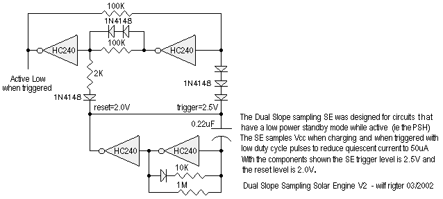
A bicore circuit was used for the oscilator to set the sample period and pulse width. This grounded bicore can control the pulse duty cycle by switching the reference voltage to the timing resistors from positive to Vcc to change the pulse output from positive to negative pulses.
The comparator uses a transistor front end to amplify the 1.2V reference voltage. The latch and the oscillator outputs connected through 200K resistors with a summed sampling voltage applied to the diode and transistor base emitter junction. The two resistors form a divide-by-two circuit so the trigger level is approximately 2 x 1.2V = 2.4V and a trigger level of 2.1V that is just 300mV lower.
Other resistor ratios should give different trigger and reset voltages. While charging, the sampling circuit analog output voltage that is applied to the left hand comparator inverter input is mostly near 0V but the circuit generates narrow pulses that approach Vcc / 2 when the trigger level is reached. Conversely, while discharging, the sampling circuit output voltage that is applied to the left hand comparator inverter input is mostly near Vcc and now the circuit generates narrow pulses that approach Vcc / 2 when the reset level is reached.
The maximum supply current
during charging is <60uA and when triggered the standby
current
is <100uA. Given the above component values, the trigger
level is 2.5V and the reset voltage is 2.0V. The reset
voltage can be lowered by increasing the value of the 2K
resistor. The circuit
works well with 4700uF to 1F capacitors
and a variety of motors.
|
|
|
|
|
|
||
|
|
This page was last updated on |
|