|
|
|
|
BEAM From the Ground Up is a BEAM Reference Library site.
Multi-junction semiconductor
devices
Transistors in all their
guises
A bit of history
Originally, devices that needed to amplify a signal (such as radios and the first computers) used the vacuum-tube amplifier. This was the original "triode": a glass tube containing a heater filament, a heated emitter plate (a.k.a., the cathode) that emits electrons, a collector plate (a.k.a., the anode) that collects the electrons once they have accelerated through the tube, and a metal grid in between. The name "triode" came from the fact that the device had three active elements -- the anode, the cathode, and the grid. Small changes to the voltage of the grid cause large changes in the electron current flowing to the collector plate. Remove the grid, and the device becomes a vacuum-tube diode.
Vacuum-tube triodes work for many purposes, but were slow, bulky, fragile, and consumed copious amounts of power. For years, researchers around the globe tried to make a solid-state version of the device in an attempt to enable the creation of smaller, faster, less power-hungry electronics. The field-effect transistor was patented by the German scientist Julius Lilienfeld in 1926, although he likely never got it to work. Meanwhile, the German physicist Robert Pohl made a solid-state amplifier in 1938 using salt as the semiconductor -- it worked, but reacted to signals too slowly to be of any use. Finally, three scientists (John Bardeen, Walter Brattain, and William Shockley) working at Bell Laboratories discovered how to make the first workable solid-state transistor on December 23, 1947.
Their first working device was a "point-contact transistor" -- Shockley's team had modified a "cat's whisker"-style diode by placing two fine metal wires close together on the surface of a piece of N-type germanium. The result could also be called a "triode", because it has three terminals -- the two free ends of the diodes and their common junction. A voltage applied to the junction controls a current flowing through the other two terminals.
Point-contact transistors, though, were essentially laboratory curiousities -- they were hard to make (performance depended on the exact placement of the wires on the germanium), and none too reliable (since they responded nearly as much to their surroundings as to their input signals). Research continued.
A month after the birth of the point-contact transistor, Shockley realised that Russell Ohl's P-type and N-type semiconductors in effect made it possible to build a solid-state analog of the vacuum tube triode. The solution was to sandwich a thin P-type semiconductor between two N-type pieces, resulting in two P-N junctions (i.e., two diodes) face to face. A current applied to the P-type layer could then control the current between the two N-type regions. The resulting bipolar transistor proved much more reliable than the point-contact transistor. In the bipolar transistor (as in all modern transistors), the vital junctions between the N-type and P-type layers are buried deep within the semiconductor crystal where they cannot be affected by their surroundings.
There are two general types of transistors in use today: (1) the bipolar transistor (often called the bipolar junction transistor, or BJT), and (2) the field-effect transistor (FET). The bipolar transistor, composed of two closely coupled P-N junctions, is bipolar in that both electrons and holes are involved in the conduction process. It is readily able to deliver a change in output voltage in response to a change in input current. This type of transistor is widely used as an amplifier and is also a key component in oscillators, high-speed integrated circuits, and switching circuits.
In contrast to the bipolar transistor, the FET is a unipolar device, its conducting process primarily involves only one kind of charge carrier. It can be built either as a metal-oxide-semiconductor field-effect transistor (MOSFET) or as a junction field-effect transistor (JFET).
Bipolar transistors
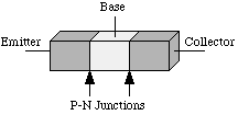
Bipolar transistors are made from 3 sections of semiconductor material (alternating P-type and N-type ), with 2 resulting P-N junctions. Schematically, a bipolar transistor can be thought of in this fashion:One PN junction is between the emitter and the base; the other PN junction is between the collector and the base. Note that the emitter and collector are usually doped somewhat differently, so they are rarely electrically interchangeable. While the terms "collector" and "emitter" go back to vacuum tube days, the base derives its name from the first point-contact transistors -- here the center connection also formed the mechanical base for the structure. In modern practice, the base region is made as thin as possible to achieve reasonable levels of current gain; it is often only about one millionth of a meter thick.
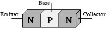
Bipolar transistors are classified as either NPN or PNP according to the arrangement of their N-type and P-type materials. Their basic construction and chemical treatment is implied by their names. That is, an NPN transistor is formed by introducing a thin region of P-type material between two regions of N-type material.
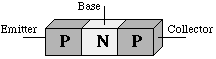
On the other hand, a PNP transistor is formed by introducing a thin region of N-type material between two regions of P-type material.
Since the majority and minority current carriers are different for N-type and P-type materials, it stands to reason that the internal operation of the NPN and PNP transistors will also be different. These two basic types of transistors along with their circuit symbols are shown here:
NPN PNP Note that the two symbols are subtly different. The vertical line represents the base (B), the angular line with the arrow on it represents the emitter (E), and the other angular line represents the collector (C). The direction of the arrow on the emitter distinguishes (graphically) the NPN from the PNP transistor. If the arrow points in, (Points iN) the transistor is a PNP. On the other hand if the arrow points out, the transistor is an NPN (Not Pointing iN).
Bear in mind that the arrow always points in the direction of hole flow (current), or from the P-type to N-type sections, no matter whether the P-type section is the emitter or base. On the other hand, electron flow is always "against" the arrow, just like in the junction diode.
As a result, a PNP transistor is "triggered" when its base is pulled low; an NPN transistor is "triggered" when its base is brought high.
Note that the bipolar transistor is a current-amplifying device, unlike the vacuum tube and the field-effect transistor (FET), both of which depend upon voltage changes to operate. It is the amount of current flowing in the base circuit that controls the amount of current flowing in the collector circuit.
Wilf Rigter has graciously contributed the following
explanation of bipolar transistor behavior in circuits:
|
|
Phototransistors
Like diodes, all transistors are light-sensitive. Phototransistors are designed specifically to take advantage of this fact. The most-common variant is an NPN transistor with an exposed base region. Here, light striking the base replaces what would ordinarily be voltage applied to the base -- so, a phototransistor amplifies variations in the light striking it. Note that phototransistors may or may not have a base lead (if they do, the base lead allows you to bias the phototransistor's light response.
Field Effect Transistors (FETs) -- JFETs, MOSFETs
A FET, or Field Effect Transistor, is yet another type of transistor -- here, the resistance between the source and drain terminals varies according to the voltage between gate and source. Higher gate-to-source voltage means less resistance.
FETs have the advantage of having an extremely low "on" resistance. They also require low gate-turn-on current. But in very low-voltage applications, they have one drawback. The average gate threshold is usually about one volt. And with a current-limiting or pulldown resistor connected to the gate, the available voltage can dip below the recommended operating conditions of the FET.
A bipolar switching transistor requires only 0.6 to 0.7 volt to turn on, giving such transistors an advantage in very-low voltage applications. In addition, most off-the-shelf FETs are generally more expensive than bipolar transistors. For the cost of a couple of FETs, you can usually purchase a bulk pack of bipolar transistors. Further, handling FETs requires much more attention than bipolar transistors, as FETs are very susceptible to damage due to static and overall experimental abuse.
|
|
|
Ben Hitchcock has a writeup on NPN transistors here, and one on PNP transistors here. Meanwhile, he also has a writeup on transistor testing here. This is great and handy stuff if you've salvaged some transistors, and their labels have been wiped off or obscured. "Iguana Labs" has a good tutorial on learning to use transistors here (just scroll down a bit). Williamson Labs has an excellent transistor tutorial here. I have a writeup on transistor usage in BEAMbots here. SatCure has a transistor tutorial here. For an illuminating comparison of the various photo-sensitive devices, make sure to check out "Choosing the Detector for your Unique Light Sensing Application." |
|
|
||
|
|
This page was last updated on |
|