|
|
The BEAM Circuits Collection is a BEAM Reference Library site.
Wilf Rigter's SIMD1 V2
Part of a family of nocturnal
solar engines (all circuits on this page ©
Wilf
Rigter ; note that the majority
of this explanatory text comes from either postings by, or
correspondence with Wilf)
Wilf's description of this design's birth:
In the never-ending quest for simplicity even one extra diode is a price I loath to pay and to avoid using extra components it struck me that the the two diodes in SIMD1 V1 were connected like the two junctions in one transistor. Eureka! replace two diodes with one transistor to restore the original component. Now one whole transistor is more than the sum of it's two diode junction parts and on closer examination, it became clear that I had fortuitously solved another problem. I wondered if the design could be made any simpler. Lo and behold SIMD1 V2 which uses one less component and doesn't require very dark conditions to turn on. The two 1N914 diodes in the earlier SIMD1 design can be replaced with a single transistor (i.e. the two diode junctions) but in the process, this revision has really enhanced the behavior.
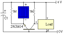
 SIMD1 V2 Basic Circuit (NPN) e = enable (active high); v = Vcc; g = Gnd |
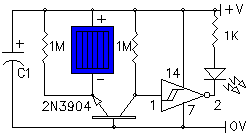
 SIMD1 V2 Example Circuit LED load with gate driving enable |
|
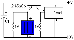
 SIMD1 V2 Basic Circuit (PNP) e = enable (active high); v = Vcc; g = Gnd |
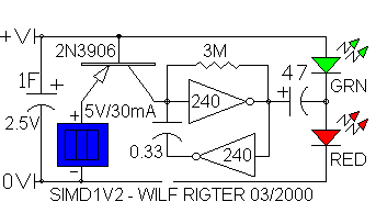
 SIMD1 V2 Example Circuit 2 Driving LED flasher circuit |
I was looking for a way to effectively speed up rate of change of the input voltage by amplifying it. When I subbed the transistor for the two diodes, I realized that the base emitter junction of the transistor was a replacement for the sensing diode, and the collector base junction provided isolation, BUT the gain of the transistor would increase the rate of voltage change on the base pin by a factor of 100 at the collector pin thereby eliminating the supply leakage problem. Since the 2N3904 replaced diodes (two in the original SIMD1 V0, one in later versions), no additional parts were required for this much improved performance.
|
|
|||
|
|
|
|
|
|
Storage capacitor |
|
|
|
|
|
|
|
|
|
|
|
|
|
|
|
|
|
|
|
2 X 1 MOhm resistors |
|
|
|
This circuit was introduced as SIMD1 V2 first shown with a Schmitt trigger driving a LED but this trivial application also required a pull-up resistor on the NPN collector. Since the NPN is on during charging, the value of the pull-up resistor is made large to reduce supply current.
A second SIMD1 V2 is shown in a more useful application where the transistor (this time without a pull-up resistor) is used to hold off a CMOS oscillator during charging which when enabled at night drives an LED pump flasher. This version really highlights the simplicity of the SIMD1 V2 design which (as in this example) can also be implemented with a PNP transistor which provides an active high signal during charging.
The PNP, which is any high gain transistor including the 2N3906, is ON during charging as the solar cell pumps current into the storage capacitor through the base emitter junction. The transistor collector clamps the input of the typical oscillator shown to +V until the solar cell output drops below the voltage of the capacitor. In my prototype, the capacitor is a 1F 2.5V gold cap charged with a simulated 5.5V solar cell and the transistor will turn off when the charging voltage drops below the fully charged capacitor voltage (~2.4V). Since the PNP operates as a common base amplifier, the voltage gain at the collector will cause a rapid voltage transition through the linear region of the 74HC240. When the PNP turns off, the oscillator starts and causes the two LEDs at the output to alternately flash. The way the 47 uf cap discharges through each LED produces a small light explosion and after-image quite pleasing to the eye.
The SIMD1 V2 design can also replace the two diodes of the original 74HC14 design or control a whole 74HC240 chip if the collector has a 1M pull down resistor to 0V and is connected to the tristate enable pins. The SIMD1 V2 prototype shown was actively flashing the 2 LEDS at a 2 Hz rate for over 4 hours on a fully charged (2.4 V) cap.
|
|
|
|
|
|
||
|
|
This page was last updated on |
|